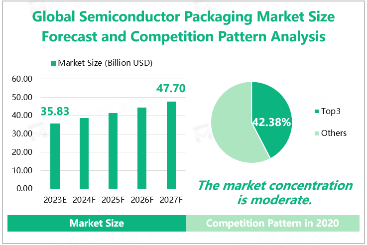
Semiconductor packaging refers to the process of processing tested wafers into independent chips according to product models and functional requirements. The specific process is as follows: the wafer from the wafer front process is cut into small chips through the wafer cutting process, and then the cut chips are glued onto the corresponding small islands of the substrate (lead frame) frame. Next, ultra-fine metal (gold tin copper aluminum) wires or conductive resin are used to connect the bonding pads of the chips to the corresponding pins of the substrate, and the required circuit is formed; Then, the independent chips are packaged and protected with a plastic shell. After plastic packaging, a series of operations are carried out. After packaging, finished product testing is carried out, usually through inspection, testing, and packaging processes, and finally stored and shipped.
Global Semiconductor Packaging Segmentation Market Analysis
From the perspective of segmentation types, the flip-chip segment market dominates. Flip chip refers to depositing tin and lead balls on I/O pads, then flipping and heating the chip. This technology combines molten tin and lead balls with ceramic substrates to replace conventional wire bonding. Currently, it is mainly used in high pulse CPUs, GPU (Graphic Processor Units), Chipset, and other products. According to our research data, the market size of the flip-chip segment is expected to reach $11.57 billion in 2023, with an estimated market share of 32.28%.
From the perspective of downstream application patterns, the consumer electronics sector is the largest downstream application market for semiconductor packaging. Data shows that the estimated application scale of semiconductor packaging in the consumer electronics field in 2023 is $22.03 billion, with a market share of 61.49%.
Global Semiconductor Packaging Market Size and Share Forecast byType and Application in 2023
|
|
Market Size (Billion USD) |
Market Share |
|
Segmented by Type |
||
|
Flip Chip |
11.57 |
32.28% |
|
Embedded Die |
0.29 |
0.81% |
|
Fan-in Wafer Level Packaging (Fi Wlp) |
1.39 |
3.89% |
|
Fan-out Wafer Level Packaging (Fo Wlp) |
0.66 |
1.83% |
|
Others |
21.92 |
61.18% |
|
Segmented by Application |
||
|
Consumer Electronics |
22.03 |
61.49% |
|
Aerospace and Defense |
1.92 |
5.35% |
|
Medical Devices |
2.35 |
6.57% |
|
Communications and Telecom |
3.64 |
10.16% |
|
Automotive Industry |
3.93 |
10.97% |
|
Others |
2.95 |
8.24% |
Source: www.globalmarketmonitor.com

For more industry information, please refer to our latest released "2023 Global Semiconductor Packaging Market Analysis Report, Key Competitors, Market Effect Factors, Growth, And Forecast".
We provide more professional and intelligent market reports to complement your business decisions.