The semiconductor industry is now transferring to mainland China, and several sputtering target manufacturers in China have expanded their production. On the 20th of December, KFMI held a groundbreaking ceremony for the industrialization project of sputtering target and key components of equipment. This project focuses on the construction of a production line for ultra-high-purity metal sputtering target and key components of large-scale equipment used in flat panel display and semiconductor. Grinm Advanced Material also has an expansion plan, and its sputtering target project is about to be completed.
A Buoyant Semiconductor Sputtering Target Market Expected
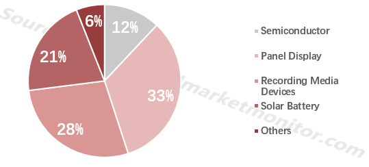
Sputtering is one of the main technologies for preparing thin film materials, and sputtering targets are indispensable raw materials in the preparation of thin film materials. A high-speed ion beam is used to bombard the surface of the sputtering target, so that the atoms on the target surface can leave the target and be deposited on the substrate surface. The main types of sputtering target are semiconductor target, magnetic recording target, photovoltaic target, display target and electronic device target. Depending on the application area, the choice of material for the sputtering target is also different.
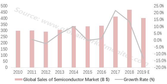
Of all the sputtering target types, the market share of semiconductor target is not the largest, but the actual market size is also considerable and growing rapidly. Affected by the negative sales growth of downstream semiconductor industry, the growth rate of the semiconductor sputtering target market has declined slightly, and global sales in 2019 is expected to reach 1.07 billion US dollars.
Application Structure of Sputtering Target

![]()
Although the sales growth rate of the semiconductor market in 2019 reached a 10-year low, due to the huge market size, the volume is still considerable. The sales of global semiconductor market in 2019 is about 400 billon US dollars, and the hotness of consumer electronics products like true wireless earbuds and 5G cellphone will maintain to the next year, and bringing the semiconductor sputtering target market back to life again.
Sales and Growth of Global Semiconductor Market

![]()
Industrial Transfer Brings Replacing Opportunity
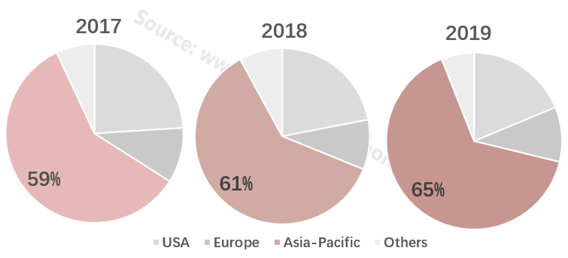
Semiconductor sputtering target industry is closely related to downstream industries, and the development of target enterprises in each region is clearly affected by the development of local semiconductor industry. The overall transfer of the semiconductor industry to the Asia Pacific region has directly driven the development of sputtering target companies there. Within the Asia-Pacific region, the semiconductor industry is trending toward mainland China, which directly brings favorable conditions for the development of Chinese semiconductor sputtering target companies.
Market Share of Semiconductor Industry

![]()
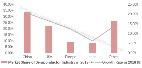
In 2018, the scale of the global semiconductor market reached 468.8 billion US dollars, and the size and growth rate of China's semiconductor market surpassed the rest of the world. Although the size of the global semiconductor market in 2019 has declined after two years of strong growth, emerging applications such as 5G will drive the growth of the semiconductor market in 2020. In the Chinese semiconductor market, which has advantages in both market share and growth rate, sputtering target companies have good prospects, and leading companies' expansion plans are already under deployment.
China Has Advantages on Both Market Share and Growth Rate

![]()
Leading Sputtering Target Enterprises in China
The industry chain of sputtering target mainly includes metal purification, sputtering target manufacturing, sputtering coating, and end-use application. Among them, sputtering target manufacturing belongs to midstream manufacturing link, and the sputtering coating is more closely related to downstream manufacturers such as foundry and panel manufacturers.
Since the sputtering targets needed by the semiconductor industry are highly purified, the technical barriers of the industry are high, and the industry presents obvious aggregation characteristics. The manufacturing of sputtering targets in the United States and Japan started earlier, and the enterprises like Honeywell, Nippon Mining, Tosoh Silica are still dominating the market.
The main sputtering target enterprises in China are KFMI, Grinm Advanced Material and Acetron. KFMI and Grinm Advanced Material are mainly engaged in semiconductor sputtering target, and the supply of both companies are still in small batches.
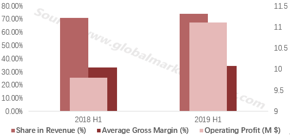
KFMI can currently supply 16nm high-end sputtering targets in batches. Although the supply volume is small, its target customers include TSMC, UMC, GLOBALFOUNDRIES, SMIC, SONY, TOSHIBA, Renesas, Micron, Hynix, STM, BOE, CSOT, SunPower and etc. According to the information disclosed by KFMI, in the first half of 2019, the sputtering target business of it is better than the same period of last year. The revenue of tantalum sputtering target, aluminum sputtering target and titanium sputtering target accounted for 73.8% of the whole revenue, and the profit of sputtering targets and relevant business reached 11.1 million US dollars, and the average gross margin of them was 34.45%.
A Contrarian Growth of KFMI Sputtering Target Business

![]()
Due to Grinm Advanced Materia’s ability to carry out vertical R&D and production integration of ultra-high-purity raw materials-sputtering targets-evaporated films, the gross margin of Grinm Advanced Materia is higher than similar companies. In 2018, the profits of high-purity and ultra-high-purity materials-related businesses alone exceeded 18.68 million US dollars. And the downstream customers of Grinm Advanced Material are first-class foundries like SMIC, TSMC, UMC and GLOBALFOUNDRIES.
We provide more professional and intelligent market reports to complement your business decisions.
 Chinese