After the commercialization of 5G network, demand for most products of 5G industry chain is growing rapidly. Since 5G mobile phone is equipped with 5G chip, the packaging and testing equipment needs to be updated, therefore manufacturers of packaging and testing equipment will get more orders in a short period of time. In the transition period from 4G to 5G, the market size of packaging and testing equipment will increase relatively.
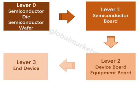
Electronic packaging steps
![]()
Semiconductor packaging is a process of forming, fixing and connecting a chip on a substrate by using techniques like thin film processing, and then potting the electronic product with a plastic insulating medium. The aim is to protect the chip from damage, ensure heat dissipation performance of the chip, and realize the transmission of electrical signals to ensure normal operation of the system.
As for semiconductor testing, this is about checking the appearance and performance of the chip for ensuring the quality of the product. As the final steps of the whole manufacturing process, semiconductor packaging and testing are extremely important finishing works.
Packaging technology is currently in the upgrade stage, and the arrival of the 5G era will accelerate the evolution of traditional packaging technology to advanced packaging technology. As the size of the 5G chip shrinks, the difficulty of packaging and testing increases. Manufacturers that do not have R&D capabilities or do not have strong financial strength to support enterprise replacements will be phased out. Also, most of the manufacturers will be merged by leading enterprises, and the concentration of the industry will be further improved.
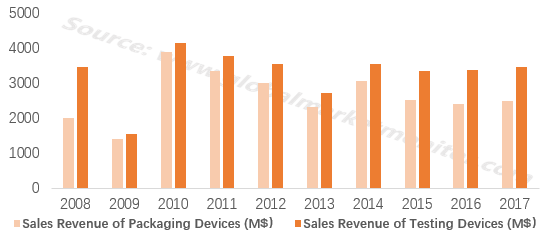
Due to the periodicity of the packaging and testing equipment (generally five years as a replacement cycle), the demand for future packaging and testing equipment is closely related to past sales. And thanks to the expansion of global semiconductor capacity, the demand for semiconductor packaging and testing equipment has increased. Following this upsurge, semiconductor packaging and testing equipment manufacturers have increased investment to expand production, and the capacity of packaging and testing equipment will be greatly improved in the next few years.
Among all the production, the production of packaging and testing equipment related to 5G is very likely to complete the digestion. But blind production, especially the production of outdated packaging and testing equipment will bring risks to the packaging equipment manufacturers.
The replacement period for equipment is coming
![]()
At present, the semiconductor packaging and testing equipment market is highly concentrated. In the next two years of replacement, smaller and failed manufacturers will be eliminated, and market concentration will be further enhanced.
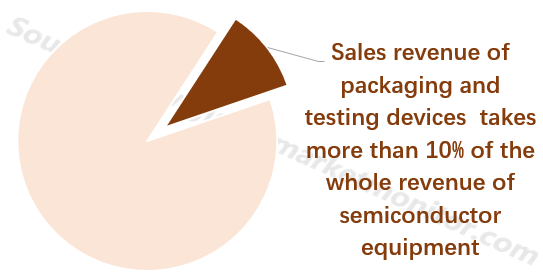
Domestic manufactures are still left behind
![]()
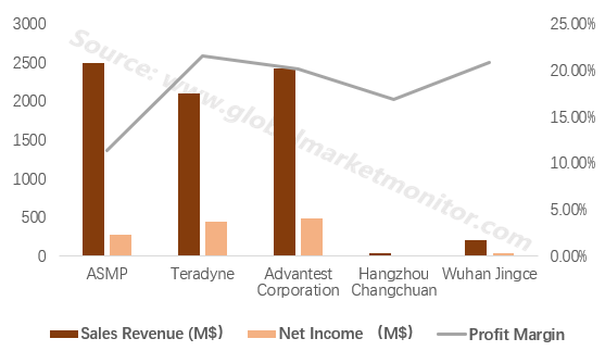
Founded in 1975 by the Dutch company ASMI in Hong Kong, ASM Pacific Technology (ASMP) is the world's largest supplier of integration and packaging equipment for the semiconductor and LED industries. ASMP has 10 manufacturing plants, 7 R&D centers, more than 1,800 R&D personnel and more than 1,100 core intellectual property rights. Thanks to the its strong production capacity and advanced technology, ASMP has maintained positive revenue growth for most years.
With a lower P/E ratio, ASMP has the greatest expectation
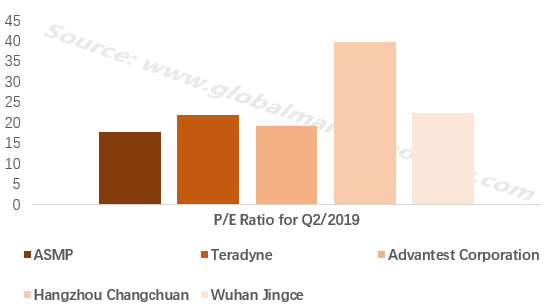
![]()
High gross margin is closely related to advanced technology
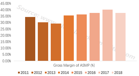
![]()
Research and development cost many in ASMP
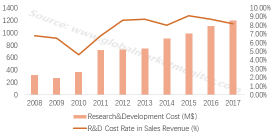
![]()
Thanks to the close ties with mainland China, ASMP has fully benefited from the development of China's semiconductor industry and will also achieve higher profits in the 5G era.
Mainland China devoted most to ASMP’s sales revenue
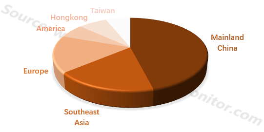
![]()
We provide more professional and intelligent market reports to complement your business decisions.
 Chinese